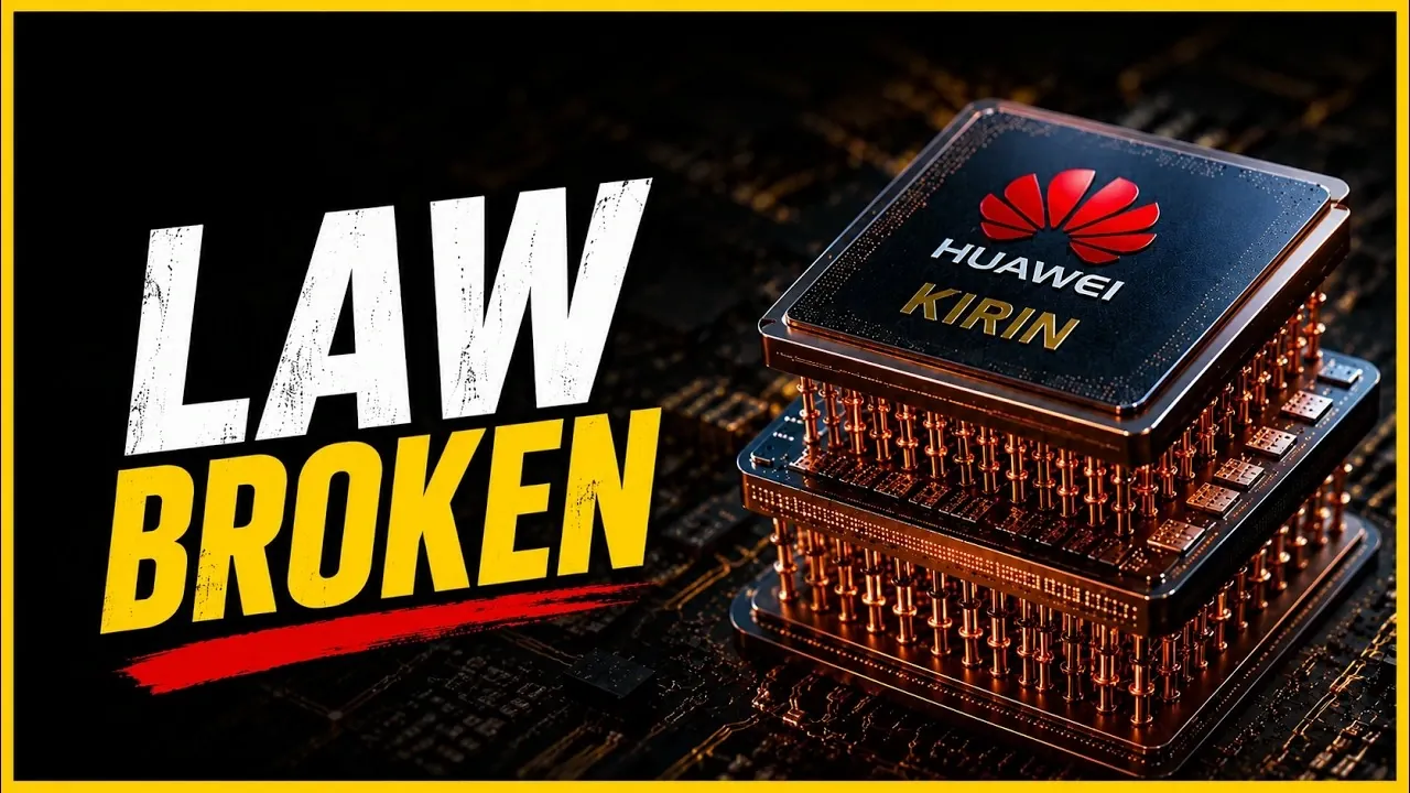
Huawei’s recent advancement in chip design, as highlighted by Two Bit da Vinci, introduces a concept known as logic folding, which addresses the limitations of Moore’s Law. By vertically stacking chip layers and incorporating Through-Silicon Vias (TSVs) for efficient interconnections, this method reduces the distance electrical signals travel. This design achieves a 41% improvement in energy efficiency and a 53% increase in transistor density, offering a tangible solution to challenges in semiconductor scaling.
Dive into the potential applications of logic folding in areas like artificial intelligence and high-performance computing. Understand the technical hurdles Huawei must overcome, including thermal management and precise layer alignment and examine the advanced cooling techniques being explored to mitigate these issues. This breakdown unpacks the engineering and practical implications of this approach for the future of chip technology.
The Decline of Moore’s Law
TL;DR Key Takeaways :
- Huawei introduced “logic folding,” a novel chip design approach that vertically stacks chip layers, improving performance and energy efficiency while addressing Moore’s Law limitations.
- The innovation is part of the “Tao Scaling Law,” which redefines chip design principles and offers a sustainable alternative to traditional transistor scaling.
- Logic folding achieves a 53% increase in transistor density and a 41% improvement in energy efficiency, using Through-Silicon Vias (TSVs) for precise vertical connections.
- Applications in AI and data centers benefit significantly, with enhanced computational efficiency, reduced energy consumption and improved scalability for high-demand workloads.
- Engineering challenges, such as thermal management and precise alignment of layers, require advanced cooling techniques and materials science breakthroughs to ensure reliability and adoption.
For decades, Moore’s Law served as the guiding principle for the semiconductor industry, predicting that the number of transistors on a chip would double approximately every two years. This trend drove exponential growth in computing power, but as transistors have approached atomic-scale dimensions, the pace of progress has slowed. Challenges such as quantum tunneling, increased heat dissipation, and the breakdown of Dennard scaling—which previously linked transistor miniaturization to energy efficiency gains, have created significant bottlenecks. These limitations have forced researchers and manufacturers to explore alternative methods to sustain advancements in computing.
What is Logic Folding?
Huawei’s “logic folding” introduces a fresh perspective on chip architecture by focusing on vertical stacking rather than solely shrinking transistors. This approach involves layering multiple chip components on top of one another, reducing the distance that electrical signals must travel. The result is faster processing speeds and improved energy efficiency. Early tests have demonstrated impressive outcomes, including a 53% increase in transistor density and a 41% improvement in energy efficiency.
The core of this innovation lies in the use of Through-Silicon Vias (TSVs), which are vertical connections that link the stacked layers. These TSVs are engineered with precision to ensure efficient alignment and minimize wasted space, making the multi-layer design both practical and effective. By using this technology, Huawei has set a new benchmark for chip design, offering a viable path forward as traditional transistor scaling reaches its physical limits.

Unlock more potential in Huawei by reading previous articles we have written.
- Can You Tell the Difference? Huawei Pura 80 Ultra vs. Pro Camera
- Mate XT Triple-Screen Folding Phone Durability Tested – Use Carefully!!
- The iPhone Fold is Real: Leaked Dummy Units Reveal Apple’s Bold New Design
- OpenAI to Launch ChatGPT 5.5 and a New Unified Desktop Super App
- Huawei Ideos U8150 Android 2.2 Phone To Launch At IFA
- Huawei Mate X folding smartphone goes on sale
- Huawei Enjoy 10e smartphone unveiled
- Honor 3C By Huawei Launched In The UK
- New Huawei Honor Tablet With 8 Inch Display Launched
- Huawei Ascend P6 Price Is 449 Euros
Scaling Beyond Traditional Limits
Vertical stacking, as demonstrated by Huawei, represents a significant departure from conventional transistor scaling. This method optimizes both spatial and temporal dimensions, allowing manufacturers to achieve higher performance without further shrinking transistors.
For instance, Huawei’s upcoming chips, such as the Comp 960, are expected to incorporate multi-layer designs that deliver unprecedented performance gains. This approach not only enhances computing power but also provides a sustainable solution for meeting the growing demands of modern applications. By addressing the limitations of traditional scaling, Huawei’s innovation could redefine the trajectory of the semiconductor industry.
Applications in AI and Data Centers
The implications of logic folding extend far beyond individual chips, offering substantial benefits for AI systems and data centers. AI workloads, which require immense computational power, stand to gain significantly from this innovation. By reducing the energy required to move data within and between chips, logic folding can make AI systems more efficient and sustainable.
In addition, advancements such as unified bus interconnects allow thousands of chips to function as a cohesive unit, further enhancing computational efficiency. Data centers, which are critical to modern digital infrastructure, can also benefit from optical data transfer between racks. This minimizes energy loss during high-speed communication, optimizing performance while reducing the environmental impact of large-scale computing operations.
Engineering Challenges and Solutions
While logic folding offers immense potential, it also introduces several engineering challenges. The TSVs that connect the chip layers must be incredibly small and precisely aligned to avoid defects or wasted space. Additionally, stacking multiple layers increases thermal density, making heat management a critical concern.
To address these issues, engineers are exploring advanced cooling techniques, including:
- High-performance heat sinks to dissipate heat efficiently
- Liquid cooling systems for enhanced thermal regulation
- Thermally conductive materials to improve heat transfer
These innovations are essential to ensure the reliability and efficiency of multi-layer chip designs. Overcoming these challenges will be key to unlocking the full potential of logic folding and allowing its widespread adoption.
The Road Ahead: Opportunities and Challenges
As the semiconductor industry confronts the physical limits of transistor miniaturization, multi-layer stacking offers a promising alternative for increasing compute density. However, this approach also adds complexity to the manufacturing process, requiring breakthroughs in materials science, fabrication techniques, and thermal management. Each additional layer introduces new challenges, from making sure precise alignment to managing heat dissipation effectively.
If these hurdles can be overcome, the potential benefits are immense. Multi-layer stacking could enable exponential growth in computing power, supporting advancements in AI, data processing and other high-demand applications. This approach provides a sustainable path forward, reducing reliance on further transistor shrinking while meeting the increasing demands of modern technology.
Implications for the Future of Computing
Huawei’s innovation in logic folding highlights how constraints can drive creative solutions. By rethinking traditional chip design, the company has opened new possibilities for efficiency, scalability, and sustainability in computing. These advancements are particularly critical for the development of AI, as energy consumption becomes an increasingly pressing concern for data centers worldwide.
As other manufacturers explore similar strategies, multi-layer stacking could become a defining feature of next-generation semiconductor technology. This shift represents more than just a technical achievement, it is a redefinition of how the industry approaches its most pressing challenges. By addressing the limitations of Moore’s Law, Huawei has laid the foundation for a new era of innovation, one that prioritizes sustainable growth and technological progress in an increasingly AI-driven world.
Media Credit: Two Bit da Vinci
Disclosure: Some of our articles include affiliate links. If you buy something through one of these links, Geeky Gadgets may earn an affiliate commission. Learn about our Disclosure Policy.